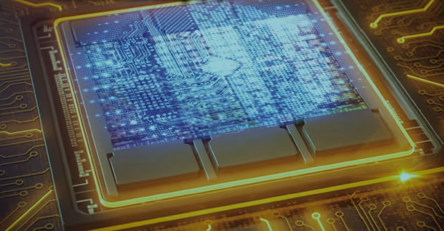
Equipment solutions enabling AI
Engineering
the Intelligent
Future
-min.avif)
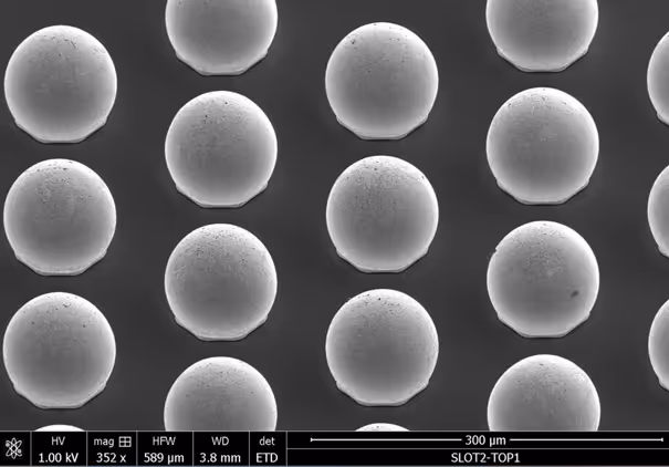
Solutions for Advanced Packaging
VeroTherm FAR can be used for Solder Balls, C4 Bumps, and µBumps needed for advanced packages.


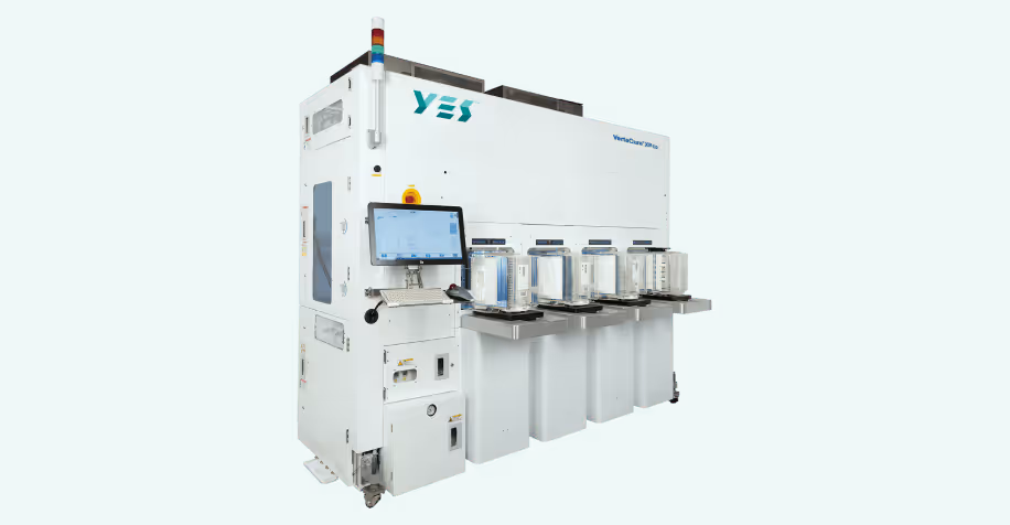
Solutions for Advanced Packaging
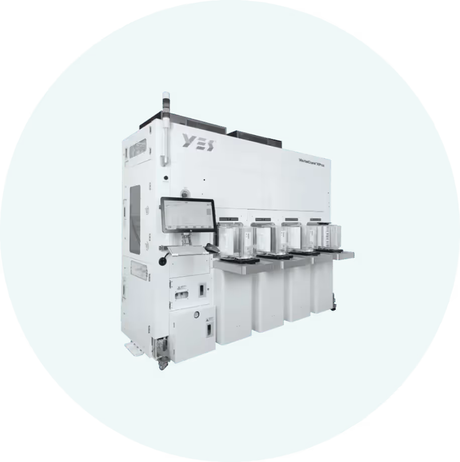
VertaCure offers a cure process for both build-up layers and the interposer.

-min.avif)
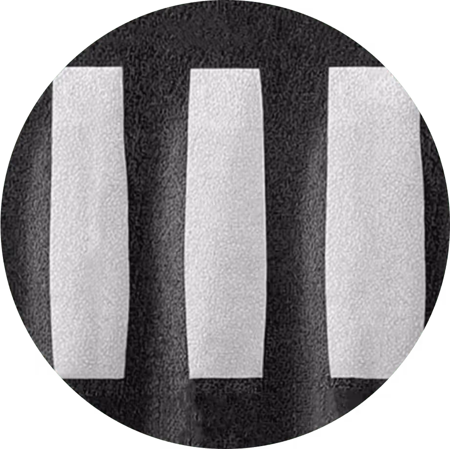
Solutions for Advanced Packaging
VertaPrime enhances the bonding needed for the build-up layers and the substrate core.

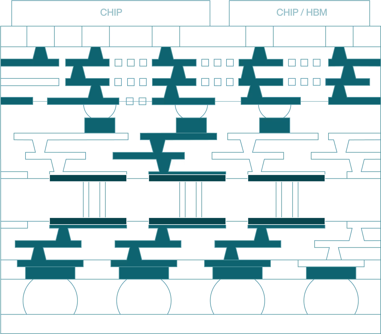
Solutions for Advanced Packaging
TersOra leverages its edge zone removal process to yield uniform edges in advanced package build-up layers.
-min.avif)
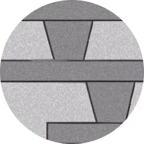
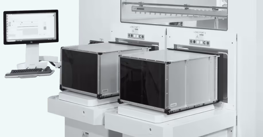
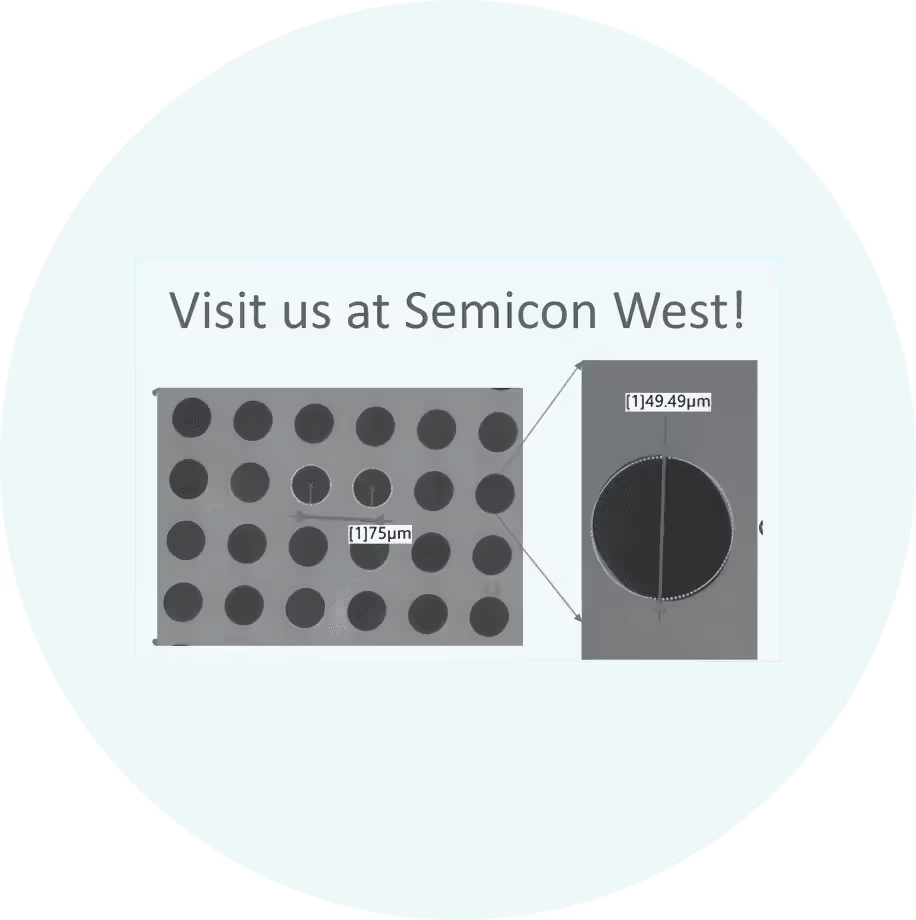
Solutions for Advanced Packaging
TersOnus Platform can be specified for precise through glass via etching in substrates for enhanced connectivity in microelectronics.

.png)
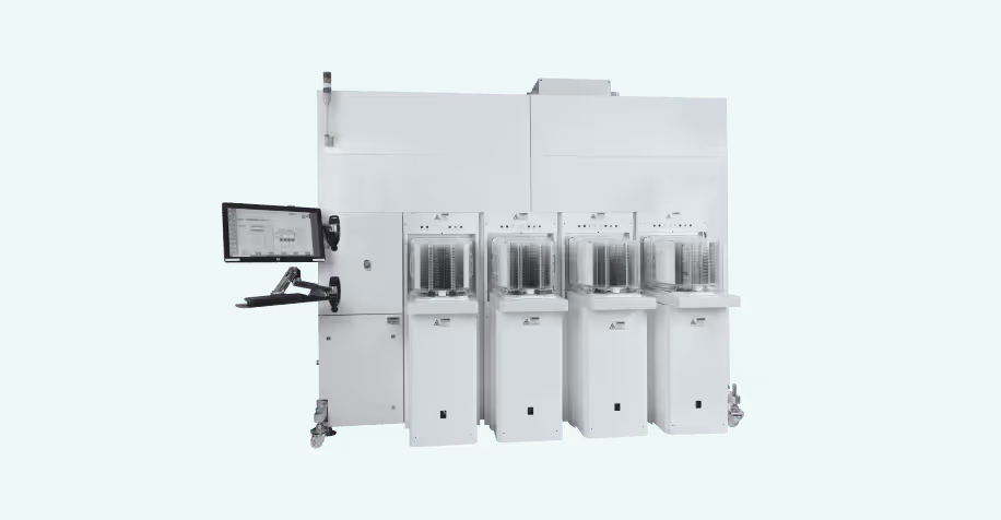
Solutions for Advanced Packaging
TersOnus Platform Electroless deposits metals critical advanced packaging build-up layers' connectivity.

.png)
.avif)
YES Announces Leadership Transition as Rezwan Lateef Appointed Chief Executive Officer
YES announced a leadership transition as the company enters its next phase of growth with top-tier semiconductor and AI computing customers. Rezwan Lateef assumes the role of CEO, succeeding Rama Alapati, who will continue in a consulting capacity to ensure continuity. Under new leadership, YES will accelerate development of next-generation advanced packaging systems and strengthen partnerships across the rapidly expanding AI and HPC markets.
YES Selected to Deliver Full Portfolio of Advanced Packaging Tools for Glass Panel AI and HPC Applications by a Leading AI Infrastructure Supplier
YES announced it has received multiple orders for its Dry and Wet process systems from a global AI infrastructure leader. The tools will support panel-level manufacturing on glass substrates for next-generation AI and HPC packaging, including curing, cleaning, reflow, and deposition solutions that enable high-throughput, glass-based 2.5D and 3D integration.
YES Receives Multiple VeroTherm™ and VeroFlex™ System Orders from Leading Memory Supplier
YES announced it has received multiple orders of its VeroTherm™ and VeroFlex™ reflow systems from a leading global memory supplier. The tools will support 3D stacking of memory and logic chips for high-performance AI accelerators, enabling sub-10 µm fluxless solder reflow with superior thermal uniformity and reliability.
.avif)
YES Receives Orders for Multiple VertaCure™ G3 Systems From Asia’s Leading Foundry
These systems will be deployed in advanced semiconductor packaging for AI and HPC, enabling precise low-temperature curing, annealing, and degassing to support next-generation 2.5D and 3D packaging technologies.
.avif)
.avif)

%20copy.avif)

-min.avif)


Corporate


Facts, numbers, and footprint
Global talent
300 employees worldwide, our staff is comprised of 220+ engineers who can deliver high-quality semiconductor products for our customers' needs.
Robust IP
With more than 100 patents, pending patents, and trade secrets, we operate on the cutting edge of technology, delivering advanced technology with our products.
Proven products
We have delivered 1,000+ tools to over 100 fabs across the world, confirming our position as an established semiconductor equipment provider.
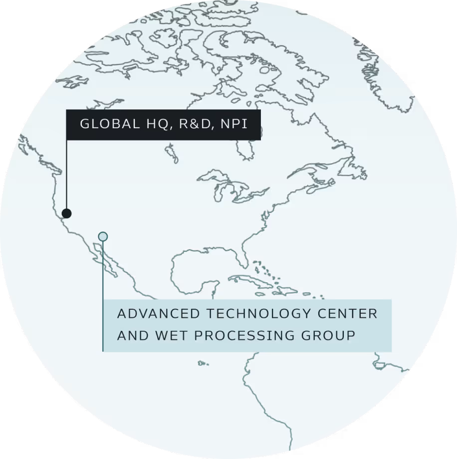
Global Footprint


Global Headquarters,
R&D and NPI
3178 Laurelview Ct. Fremont, CA 94538
+1 (510) 954-6889
Advanced Technology Center and Wet Processing Group
3200 W. Germann Rd. Chandler, AZ 85286
+1 (602) 740-7179
Manufacturing
SF No. 253, No. 96/3, Vadakku Sambala Thottam Kannampalayam, Sulur Taluk, Tamil Nadu 641402, India
+1 (888) 937-3637
Engineering and R&D
Export Promotion Industrial Park 8 Crystal Kalyani Platina, EPIP Zone, Brookefield, Bengaluru, Karnataka 560037, India
+1 (888) 937-3637B-6, 1st Floor, Elysium Central, Puliakulam Rd
+1 (888) 937-3637
Ramaliga Chettiyar Layout, Coimbatore, Tamil Nadu
641045, India
Sales & Service
7F.-2, No. 6, Taiyuan 1st St., Zhubei City, Hsinchu County 302082, Taiwan
+1 (888) 937-3637a1508, 27 Dongtancheomdansaneop 1-ro, Hwaseong-si,
+1 (888) 937-3637
Gyeonggi-do, 18469 South Korea3-28-12 Meieki, Nakamura Ward, Nagoya, Aichi 450-0002,
+1 (888) 937-3637
JapanWestendstraße 28, 60325 Frankfurt am Main Germany
+1 (888) 937-3637
